SKU:3889218
New
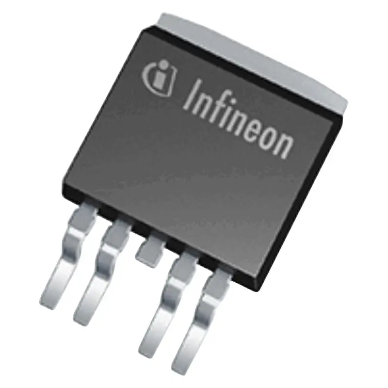
Image is for illustrative purposes only
The BTS426L1 is a high-performance N-channel vertical power FET, developed using advanced Smart SIPMOS technology. This intelligent high-side power switch is designed to provide seamless diagnostic feedback and a suite of embedded protection functions, making it a reliable alternative to traditional electromechanical relays and discrete circuits.
Equipped with comprehensive protection features, the device ensures system safety through overload protection, current limitation, and short circuit protection. It also includes thermal shutdown and overvoltage protection, which covers load dump scenarios. The switch is specifically optimized for fast demagnetization of inductive loads and offers robust protection against reverse battery connection, loss of ground, and electrostatic discharge (ESD).
This microcontroller-compatible switch is versatile enough to handle all types of resistive, inductive, and capacitive loads in 12 V and 24 V DC grounded systems. Its open-drain diagnostic output allows for efficient monitoring, including open load detection in the ON-state. Furthermore, the BTS426L1 is an environmentally friendly choice, being Green Product (RoHS compliant) and AEC Qualified for automotive-grade reliability.
Overvoltage protection Vbb(AZ): 43 V
Operating voltage Vbb(on): 5.0 ... 34 V
On-state resistance RON: 60 mΩ
Nominal load current (ISO) IL(ISO): 7.0 A
Current limitation IL(SCr): 16 A
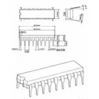
Package type: PG-TO263-5-2
Pin 1 (GND): Logic ground
Pin 2 (IN): Input, activates switch on logical high signal
Pin 3 (Vbb): Positive power supply voltage (shorted to tab)
Pin 4 (ST): Diagnostic feedback, low on failure
Pin 5 (OUT): Output to the load
Supply voltage (max): 43 V
Supply voltage for short circuit protection: 34 V
Load dump protection (VLoadDump): 60 V
Operating temperature range (Tj): -40 ... +150 °C
Storage temperature range (Tstg): -55 ... +150 °C
Power dissipation (DC, TC ≤ 25 °C): 75 W
Inductive load switch-off energy dissipation (EAS): 0.74 J
Electrostatic discharge (ESD) capability (Input): 1.0 kV
Electrostatic discharge (ESD) capability (Other pins): 2.0 kV
Input voltage (DC): -10 ... +16 V
Thermal resistance chip - case (RthJC): 1.67 K/W
Thermal resistance chip - ambient (RthJA): 75 K/W (34 K/W on SMD PCB)
Turn-on time to 90% VOUT: 80 - 400 µs
Turn-off time to 10% VOUT: 80 - 450 µs
Slew rate on (10 to 30% VOUT): 0.1 - 1 V/µs
Slew rate off (70 to 40% VOUT): 0.1 - 1 V/µs
Undervoltage shutdown: 3.5 - 5.0 V
Overvoltage shutdown: 34 - 43 V
Standby current (Vbb off): 10 - 25 µA
Initial peak short circuit current limit (Tj = 25°C): 25 A
Thermal overload trip temperature: 150 °C
Open load detection voltage (off-condition): 2 - 4 V
Input turn-on threshold voltage: 1.7 - 3.5 V
Input resistance: 2.5 - 6 kΩ
Operating voltage Vbb(on): 5.0 ... 34 V
On-state resistance RON: 60 mΩ
Nominal load current (ISO) IL(ISO): 7.0 A
Current limitation IL(SCr): 16 A
Package type: PG-TO263-5-2
Pin 1 (GND): Logic ground
Pin 2 (IN): Input, activates switch on logical high signal
Pin 3 (Vbb): Positive power supply voltage (shorted to tab)
Pin 4 (ST): Diagnostic feedback, low on failure
Pin 5 (OUT): Output to the load
Supply voltage (max): 43 V
Supply voltage for short circuit protection: 34 V
Load dump protection (VLoadDump): 60 V
Operating temperature range (Tj): -40 ... +150 °C
Storage temperature range (Tstg): -55 ... +150 °C
Power dissipation (DC, TC ≤ 25 °C): 75 W
Inductive load switch-off energy dissipation (EAS): 0.74 J
Electrostatic discharge (ESD) capability (Input): 1.0 kV
Electrostatic discharge (ESD) capability (Other pins): 2.0 kV
Input voltage (DC): -10 ... +16 V
Thermal resistance chip - case (RthJC): 1.67 K/W
Thermal resistance chip - ambient (RthJA): 75 K/W (34 K/W on SMD PCB)
Turn-on time to 90% VOUT: 80 - 400 µs
Turn-off time to 10% VOUT: 80 - 450 µs
Slew rate on (10 to 30% VOUT): 0.1 - 1 V/µs
Slew rate off (70 to 40% VOUT): 0.1 - 1 V/µs
Undervoltage shutdown: 3.5 - 5.0 V
Overvoltage shutdown: 34 - 43 V
Standby current (Vbb off): 10 - 25 µA
Initial peak short circuit current limit (Tj = 25°C): 25 A
Thermal overload trip temperature: 150 °C
Open load detection voltage (off-condition): 2 - 4 V
Input turn-on threshold voltage: 1.7 - 3.5 V
Input resistance: 2.5 - 6 kΩ