SKU:MOC8101

Image is for illustrative purposes only
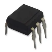
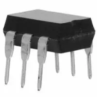
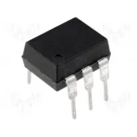
The MOC8101 optocoupler provides reliable signal transmission between electrically isolated circuits, ensuring safety and performance in sensitive applications. It features a gallium arsenide infrared emitting diode optically coupled to a silicon planar phototransistor detector and comes in a plastic plug-in DIP-6 package.
General Information
The MOC8101 ensures that the potential difference between circuits does not exceed the maximum permissible reference voltages. The absence of a base terminal connection enhances common mode interference immunity.
Key Features
- Isolation test voltage: 5300 VRMS
- No base terminal connection for improved common mode interface immunity
- Long term stability
- Industry standard dual in line package
- Compliant to RoHS Directive 2002/95/EC and in accordance to WEEE 2002/96/EC
Agency Approvals
- UL1577, file no. E52744 system code H or J, double protection
- CSA 93751
- BSI IEC 60950; IEC 60065
- DIN EN 60747-5-5 (VDE 0884) available with option 1
Applications
The MOC8101 is well-suited for applications requiring electrical isolation between circuits. It effectively protects sensitive control circuits from high-voltage transients, ensuring safety and reliable performance in power supplies and various control systems.
Package Dimensions
The MOC8101 is available in a DIP-6 package with dimensions designed for easy integration into circuit boards. Detailed measurements can be found in the datasheet.
Manufacturer Information
The MOC8101 is manufactured by Vishay Semiconductors, a subsidiary of Vishay Intertechnology, specializing in power MOSFETs, IGBTs, and other power semiconductors. Other manufacturers include Onsemi/Fairchild and Motorola.
Isolation Test Voltage: 5300 VRMS
Continuous Forward Current: 60 mA
Surge Forward Current (t≤10 µs): 2.5 A
Reverse Voltage: 6.0 V
Collector-Emitter Breakdown Voltage: 30 V
Emitter-Collector Breakdown Voltage: 7.0 V
Collector Current: 50 mA
Collector Current (t≤1.0 ms): 100 mA
Storage Temperature Range: –55 to +150°C
Ambient Temperature Range: –55 to +100°C
Junction Temperature: 100°C
Soldering Temperature (max. 10 s, dip soldering: distance to seating plane ≥1.5 mm): 260°C
Creepage: ≥7.0 mm
Clearance: ≥7.0 mm
Isolation Thickness between Emitter and Detector: ≥0.4 mm
Comparative Tracking Index per DIN IEC 112/VDE 0303, part 1: 175
Isolation Resistance (VIO=500 V): ≥10^12 Ω
Forward Voltage: 1.5 V
Maximum Collector Emitter Saturation Voltage: 400 mV
Number of Channels: 1 Channel
If - Forward Current: 100 mA
Current Transfer Ratio: 50-80 % @ 10mA
Rise Time: 2 us
Fall Time: 2 us
Height: 3.81 mm
Length: 8.7 mm
Width: 6.5 mm
Power Dissipation: 250 mW
-
 91298639.17 €Customer price8.71 €-5%